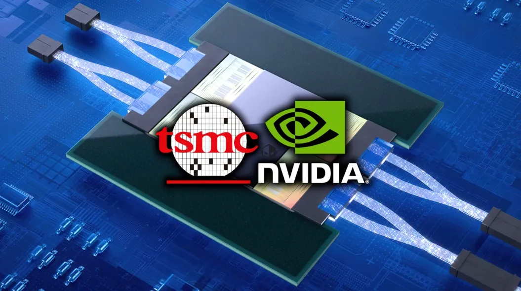
NVIDIA and TSMC, industry leaders in AI and semiconductor manufacturing, have reportedly developed a groundbreaking silicon photonics-based chip prototype.
This innovation, detailed in a recent Taiwanese press report, marks a significant step forward in overcoming the physical limitations of traditional semiconductor fabrication.
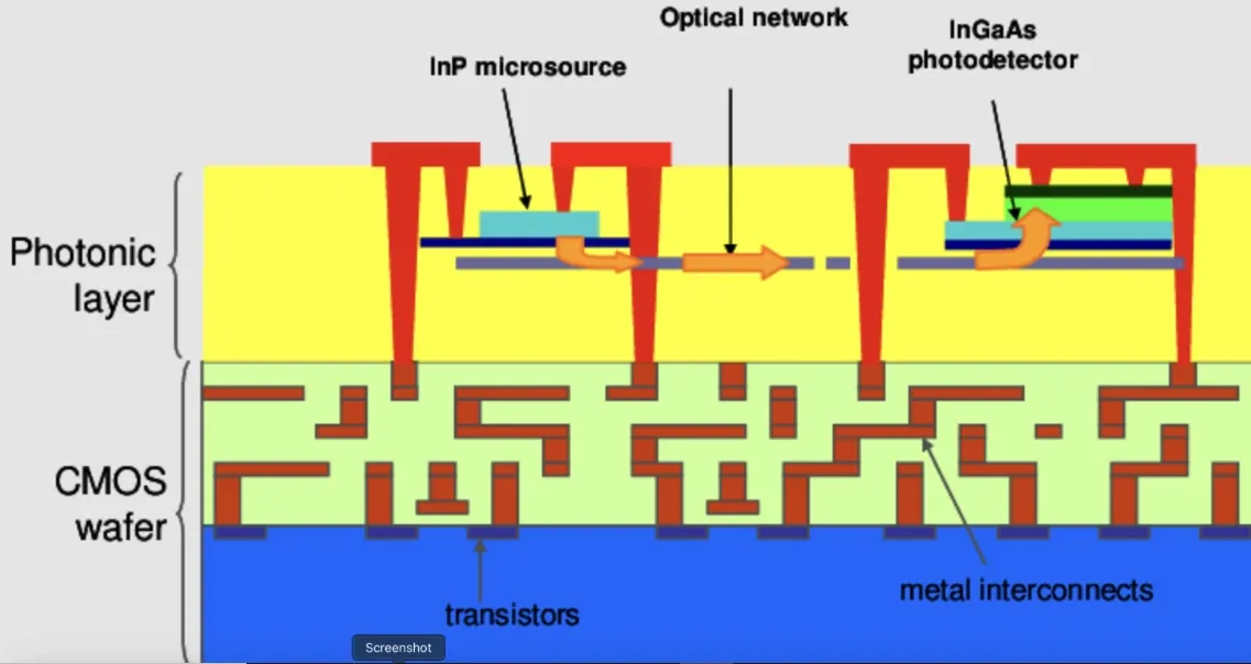
Silicon Photonics
Silicon photonics is an emerging chip manufacturing technology that integrates photonic circuits with traditional ones.
This approach replaces electrons with photons for communication within a chip, enabling faster data speeds and higher processing volumes without requiring significantly advanced manufacturing techniques.
Key Features of Silicon Photonics:
-
Photonic Transistors: Use photons for communication, allowing greater bandwidth and frequency.
-
Enhanced Data Processing: Achieves higher speeds and volumes for AI and other data-intensive applications.
-
Compatibility: Works alongside traditional circuits, enabling seamless integration.
This technology addresses the challenges of scaling down transistor sizes while maintaining performance, making it a key focus as the industry faces diminishing returns from traditional chip advancements.
NVIDIA and TSMC
According to the report, NVIDIA and TSMC developed their first silicon photonics chip prototype late last year.
The collaboration extends to advanced packaging technologies and optoelectronic integration, both critical for improving AI chip performance.
Advanced Packaging and Optoelectronic Integration:
-
Optoelectronic Integration: Combines light-managing components (e.g., lasers, photodiodes) with electronic components (e.g., transistors) on the same wafer.
-
Nanometer Node Technology: TSMC’s advanced node features minimum gate and metal pitches of 45 and 20 nanometers, respectively, pushing the boundaries of semiconductor design.
These advancements are crucial in addressing industry constraints, such as limited packaging capacity and high costs, while solidifying NVIDIA’s position as a leader in AI chip performance.
Industry Implications
The development of silicon photonics and advanced packaging technologies represents a paradigm shift in semiconductor design, offering solutions to longstanding challenges in chip manufacturing.
Potential Benefits:
-
Increased chip performance and efficiency.
-
Reduced reliance on traditional scaling methods.
-
Enhanced AI capabilities through faster and more reliable processing.
As NVIDIA and TSMC continue to pioneer these technologies, the collaboration underscores the transformative potential of silicon photonics in shaping the future of semiconductors and AI innovation.